
Education, Educational articles
Blind Vias vs Through-Hole Vias in PCB Design
Sep
Introduction: The Critical Role of Vias in PCB Design
Printed circuit boards (PCBs) form the backbone of modern electronics. Whether you are designing smartphones, IoT devices, 5G modules, or industrial controllers, the design of vias—the tiny copper-plated holes that connect layers—can significantly affect performance, cost, and reliability.
One of the most important decisions in multilayer PCB design is choosing between blind/buried vias and through-hole vias. At first glance, vias may seem like a minor detail, but the choice directly influences signal integrity, routing density, manufacturing yield, and overall product success.
In this article, we will explore the differences between blind/buried vias and through-holes, their advantages and disadvantages, fabrication considerations, and when to choose one over the other. By the end, you’ll have a clear framework for selecting the right via strategy for your PCB projects.
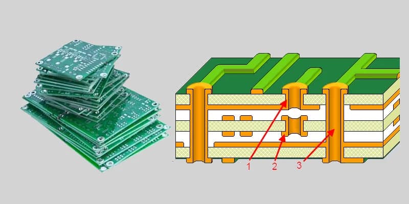
What Are Vias in PCB Design?
A via is a conductive pathway that connects different layers of a PCB by drilling a hole and plating it with copper. Without vias, it would be impossible to interconnect traces across multiple layers.
There are three major types of vias used in multilayer PCB design:
- Through-Hole Vias (THV): Drilled completely from the top to the bottom layer.
- Blind Vias: Connect an outer layer to one or more inner layers but do not go through the entire PCB.
- Buried Vias: Connect only inner layers and are not visible from the outer surface.
Each via type has unique benefits and trade-offs, which we’ll analyze in detail.
Through-Hole Vias: The Traditional Workhorse
Advantages
- Simplicity of Manufacturing: Through-holes are the most straightforward vias to fabricate, requiring only standard drilling and plating processes.
- Lower Cost: Since the process is mature and yields are high, through-holes are generally cheaper than blind or buried vias.
- Mechanical Strength: Through-holes provide strong mechanical support, especially in thicker boards or connectors where structural integrity matters.
Disadvantages
- Routing Limitations: Because through-holes pass through all layers, they consume routing space even where they aren’t needed.
- Stub Effect: At high frequencies, unused via stubs act as parasitic elements, degrading signal integrity in high-speed or RF designs.
- Larger Form Factor: Through-holes are less suited for today’s ultra-compact devices where every square millimeter counts.
Best Use Cases
- Standard multilayer boards (4–8 layers).
- Cost-sensitive applications like consumer electronics.
- Boards where mechanical durability outweighs miniaturization.
Blind and Buried Vias: Enabling HDI and High-Speed Design
Blind Vias
Blind vias start from an outer layer and end at one or more inner layers. They don’t extend through the entire PCB, saving routing space and reducing stub length.
Buried Vias
Buried vias connect only inner layers and are completely hidden inside the board. These maximize surface area on the outer layers for components and routing.
Advantages
- Higher Routing Density: Essential for HDI (High Density Interconnect) PCBs used in smartphones, wearables, and 5G systems.
- Better Signal Integrity: By reducing stub length, blind/buried vias improve performance in high-frequency and high-speed designs.
- Compact Designs: Freeing up space enables thinner, smaller boards for portable devices.
Disadvantages
- Complex Fabrication: Requires sequential lamination, laser drilling, or advanced processes, which increase manufacturing time.
- Higher Cost: Blind/buried vias can cost 2–3 times more than through-hole boards.
- Lower Yield: More steps in fabrication lead to higher risks of defects, affecting yield and reliability.
Best Use Cases
- HDI PCBs where miniaturization is critical.
- High-frequency circuits (RF, 5G, Wi-Fi 6).
- Products with strict size constraints, like smartphones, tablets, and medical wearables.
Signal Integrity and Electrical Performance
Signal integrity is one of the biggest reasons engineers prefer blind or buried vias over through-holes in advanced designs.
- Through-Holes: The longer stub length introduces unwanted capacitance and inductance. This can cause reflections, crosstalk, and attenuation in high-speed signals.
- Blind/Buried Vias: Shorter paths reduce parasitic effects, making them ideal for designs above 5–10 GHz.
For high-speed differential pairs and impedance-controlled traces, blind/buried vias offer significant advantages.
Cost Considerations in PCB Via Selection
Cost is often the deciding factor between via types.
- Through-Hole Boards: Cheapest to manufacture due to established processes.
- Blind/Buried Via Boards: Significantly more expensive due to additional drilling, lamination, and yield risks.
Rule of Thumb:
- If the design can tolerate through-hole stubs and routing limitations, choose through-holes.
- If performance and miniaturization are critical, blind/buried vias are worth the investment.
Reliability and Yield
- Through-Holes: Extremely reliable with decades of proven performance. Lower risk of open circuits or plating issues.
- Blind/Buried Vias: Require precise alignment and plating. Manufacturing yield is lower, especially for complex layer stacks.
For mission-critical systems (aerospace, automotive safety), designers often prefer through-holes unless absolutely necessary.
Manufacturing Techniques
- Drilling
- Through-holes: mechanical drilling.
- Blind/buried: often require laser drilling for microvias.
- Lamination
- Through-holes: single lamination.
- Blind/buried: sequential lamination cycles, which increase time and cost.
- Inspection and Testing
- Advanced inspection required for blind/buried vias to ensure plating quality.
Which Via Type Should You Choose?
The decision between blind/buried vias and through-holes is not about “better or worse.” It’s about matching design priorities:
- Choose Blind/Buried Vias if:
- You need miniaturization and HDI density.
- Your design operates at high frequencies where signal integrity matters.
- Cost is less critical than performance.
- Choose Through-Holes if:
- You need mechanical robustness and proven reliability.
- Cost efficiency is a priority.
- The design does not involve ultra-high-speed signals.
Industry Applications
- Smartphones & Tablets: Blind/buried vias for ultra-compact HDI designs.
- 5G and RF Modules: Blind vias for high-frequency performance.
- Automotive Electronics: Through-holes for reliability under harsh conditions.
- Industrial Equipment: Through-holes for durability and cost efficiency.
Future Trends in PCB Via Technology
- Microvias and stacked vias are becoming more common in cutting-edge HDI boards.
- Hybrid via strategies (mixing through-holes with blind/buried) balance cost and performance.
- As IoT and 5G expand, blind/buried vias will dominate compact, high-speed consumer devices.
Conclusion
In multilayer PCB design, via selection is a critical engineering choice. Blind and buried vias enable high-density, high-speed designs but come at higher cost and complexity. Through-hole vias, on the other hand, remain reliable, cost-effective, and suitable for many applications.
The best engineers don’t see the choice as “blind vs. through-hole” but as a design trade-off—balancing signal integrity, manufacturability, cost, and reliability.
By understanding the strengths and weaknesses of each via type, you can make informed decisions that align with your project’s goals, whether that’s cutting-edge 5G smartphones or robust industrial controllers.